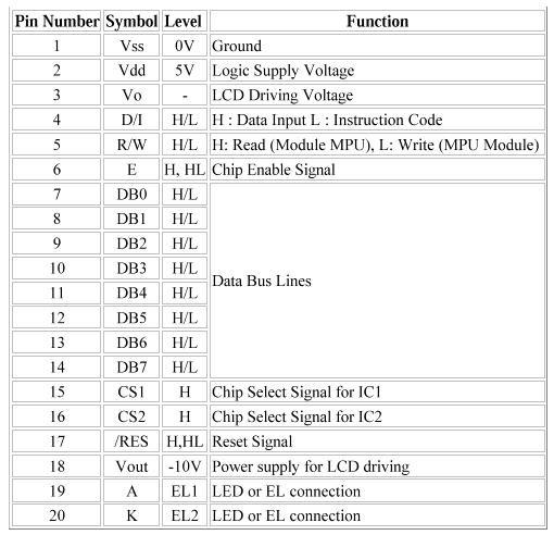
Overall structure: 128*64 array of pixels, split into left and right halves each driven by identical column driver chips. These chips are what the micro talks to via a parallel bus, they contain the video RAM. (You can forget about the row driver chip, it just drives the rows.)
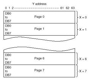
Memory structure: There are 512 bytes of memory in each chip (for 64*64 pixels). Bit zero of address zero is the top left hand corner of the 64*64 array for the particular chip. Bit one is the pixel below that, and so on up to bit 7 (ie the byte is arranged vertically). Bytes 1 to 63 are repeated to the right, forming a block of pixels 64 across by 8 down. The next 64 bytes (64 to 127) form another 64 * 8 block immediately below that. This continues for 8 blocks of 64 bytes, ie 64*64 pixels. A bit high is "light on".
Two modifiers: A software accessible "Z" register can take on values from 0 to 63. This sets the start line of the display, ie if it is set to 4 then the top of the display starts at the 5th line in the picture above, continues down to the 64th line, then wraps round to display lines 1 to 4 (ie all the data is displayed). There is also an "ADC" pin on the chip hardwired into the display board which can reverse the order of the columns in this picture.
Memory addressing: The 9 bit address is split into 3 MSBs which are a page (or X) address, and 6 LSBs which are the column (or Y) address. The page/X address selects one of the eight "64 across by 8 down" pixel blocks mentioned above. There are commands to read and write this address. The Y address selects the vertically arranged bytes 0 to 63 corresponding to the 64 columns from left to right. There are commands to read and write the Y address, additionally when a byte is accessed, the address automatically increments by one (and wraps around if necessary, but doesn't affect the X page).
NOTE: What the chip datasheet calls the X and Y addresses, really corresponds to y and x display co-ordinates. Don't let this confuse you.
Bus structure: There are 8 datalines, an instruction/command input line, a read/write input line, and a chip select for each chip (ie left or right half of screen). Commands or data are asynchronously clocked in or out of the display module depending on the settings of these signals, by an enable line.
These commands are as follows...
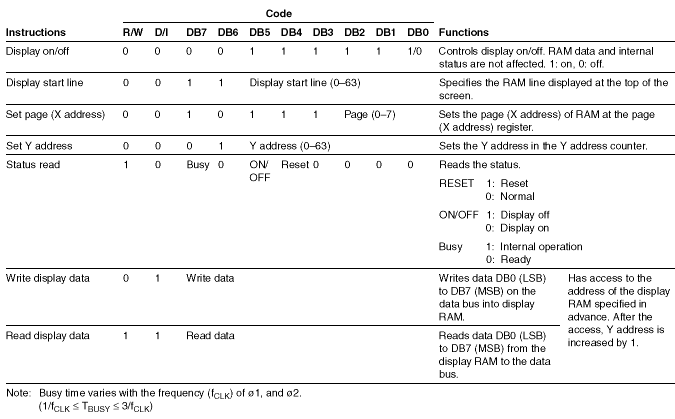
After issuing a command, the busy bit can be polled until it goes to zero, or the phase clock of the chips measured (scope) and at least 3 clock cycles allowed for each command.
Lines to play with:
Connect the 6 control lines to an output port (at least 2 lines are dedicated to the display).
Connect the 8 data bus lines to an I/O port.
For a write to display command, E starts low. R/W, CSx and D/I need to be setup for at least 140ns before E is set high for at least 450ns. Data must be ready on DB0-DB7 at least 200ns before the falling edge of E which clocks in the data. The control and data lines need to be held for 10ns after the falling edge of E. E must stay low for at least 450ns, and the total cycle time of E should not exceed 1000ns.
In other words, for a micro - set up control lines, raise E, write setup data, lower E, repeat
For a read from display command, E starts low. R/W, CSx and D/I need to be setup for at least 140ns before E is set high, which clocks out the data after at most 320ns. At least 450ns after E was set high, E can be lowered and data will hold for a minimum of 20ns. The control and data lines need to be held for 10ns after the falling edge of E. E must stay low for at least 450ns, and the total cycle time of E should not exceed 1000ns.
In other words, for a micro - set up control lines, raise E, read data, lower E, repeat
A dummy read is needed immediately after the column address is set.
I assume the busy bit isn't updated asynchronously, so repeated "read" bus cycles will be necessary.
The reset can be relied on to set the Z address (display start line) to zero and turn the display off.
Additional pins: